Semiconductor
Semiconductor Fab Ultra-pure Water Plant
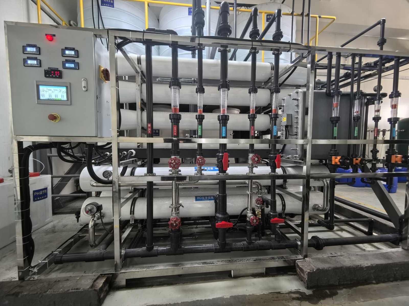
Two-stage RO + EDI + polishing loop supplying wafer cleaning lines with 18.2 MΩ·cm ultra-pure water.
Challenge
Project Requirements
Wafer rinsing required stable 18 MΩ·cm water with TOC below 10 ppb and virtually no particles, while the existing mixed-bed plant produced fluctuating quality and generated acid-alkali regeneration waste.
Engineered Solution
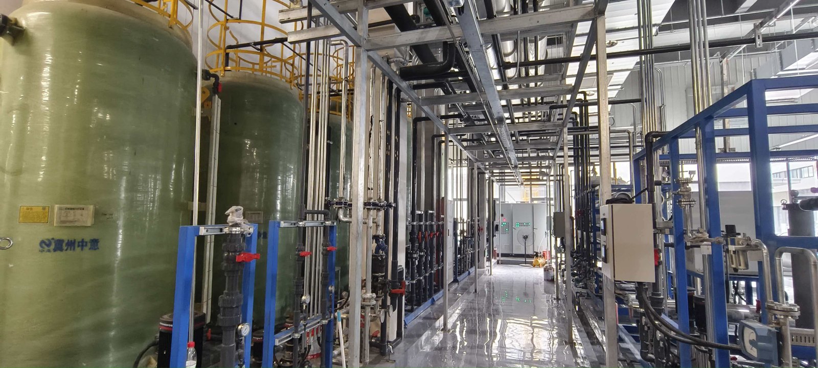
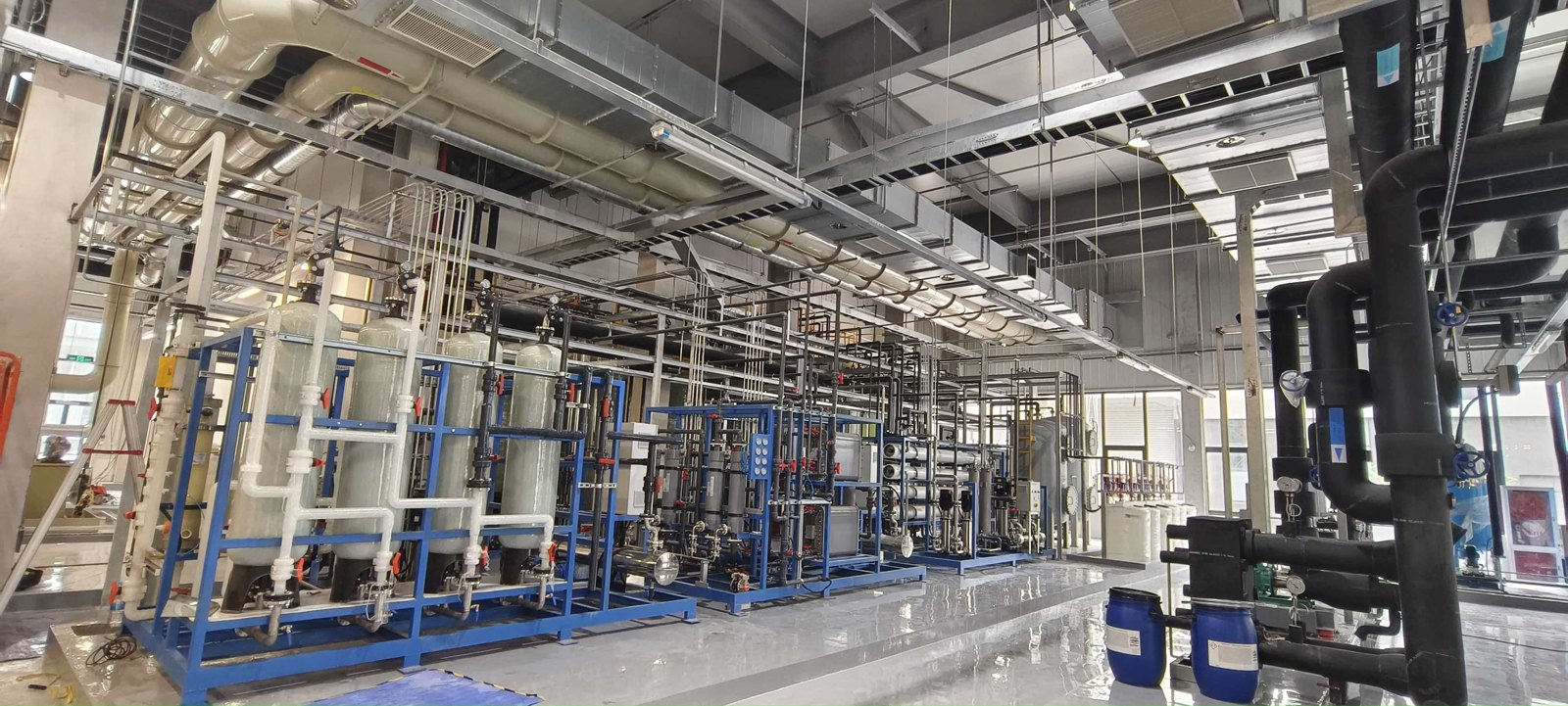
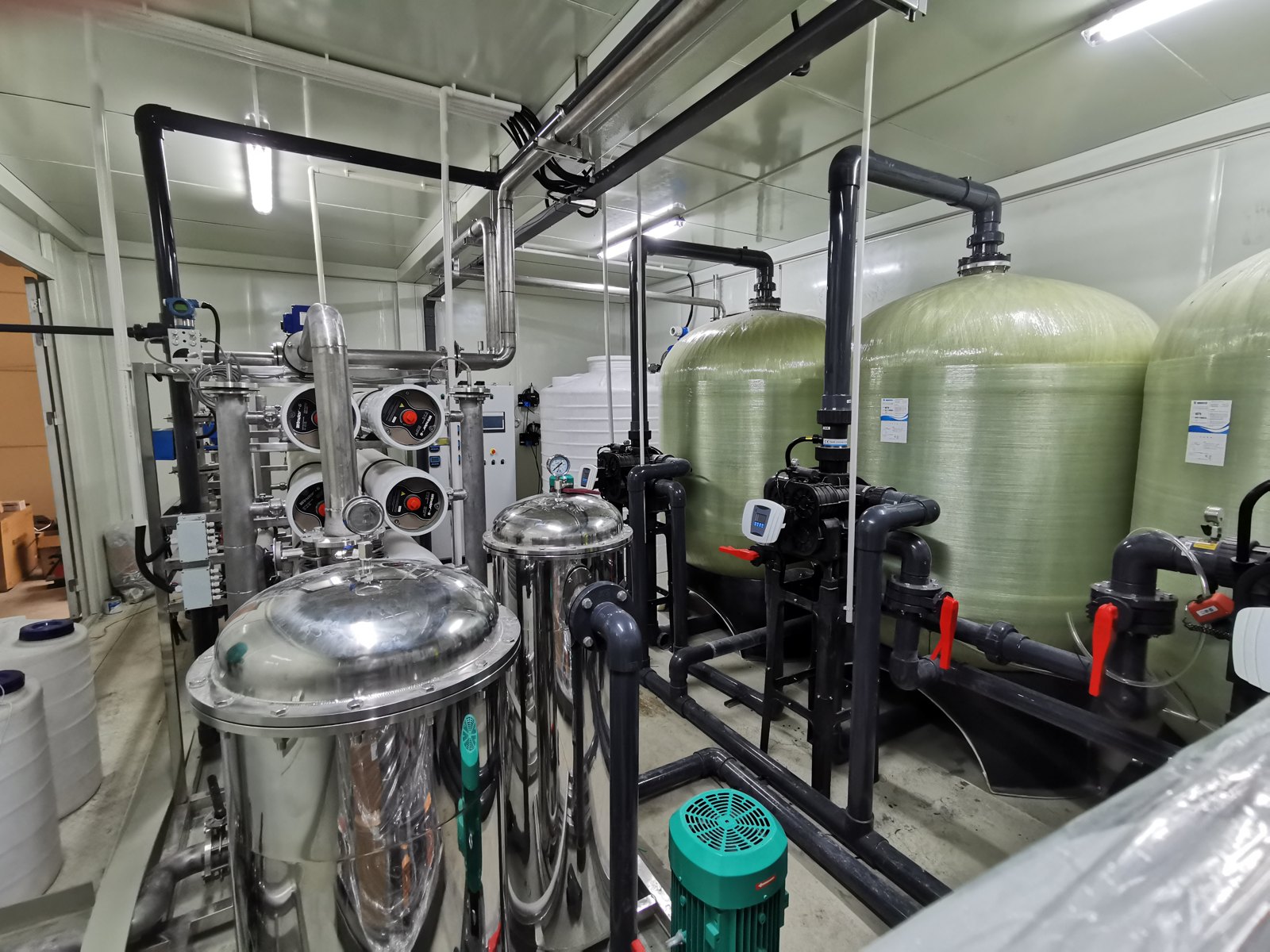
- Multi-media, activated carbon and softening pre-treatment sized for peak demand
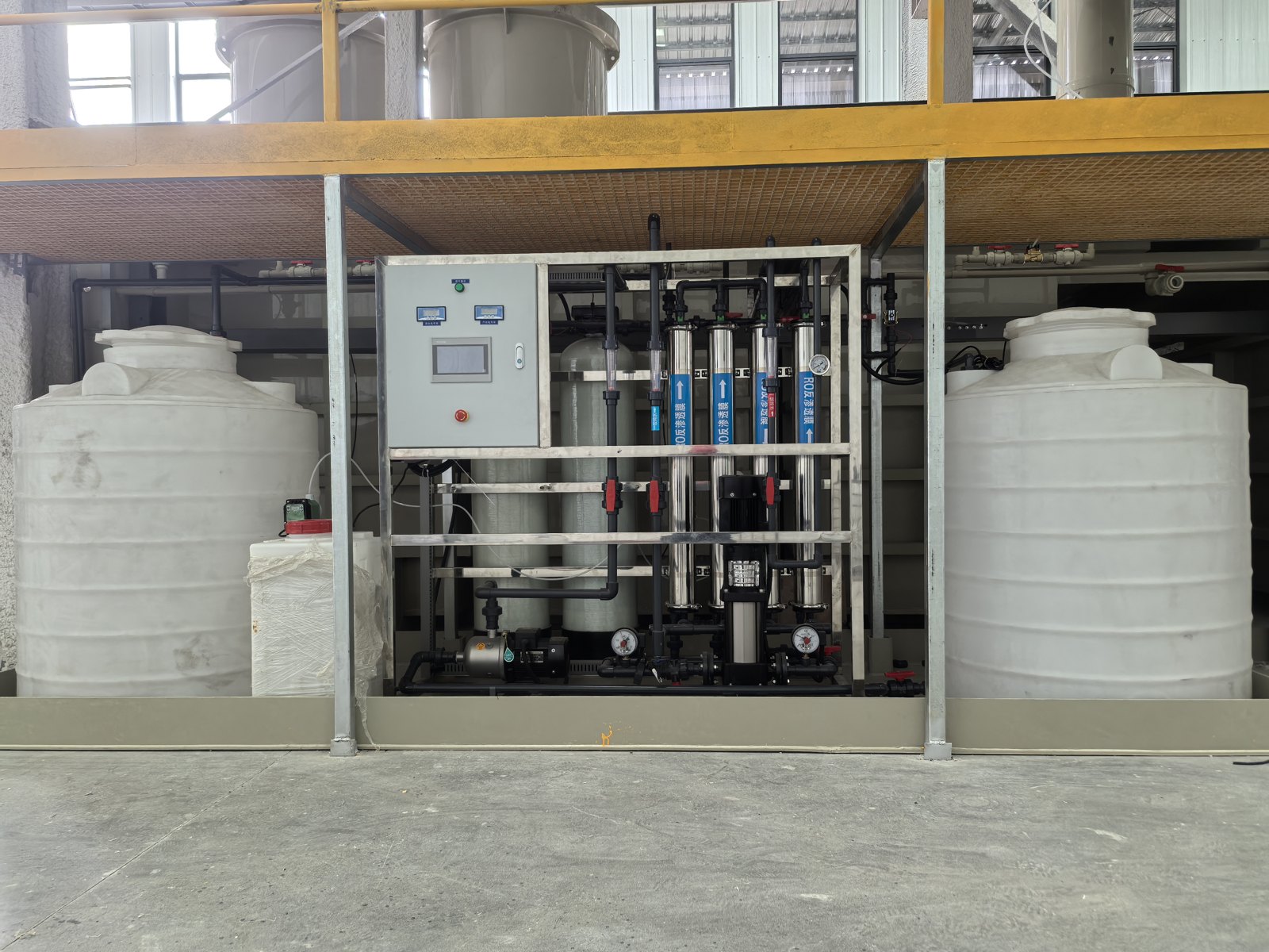
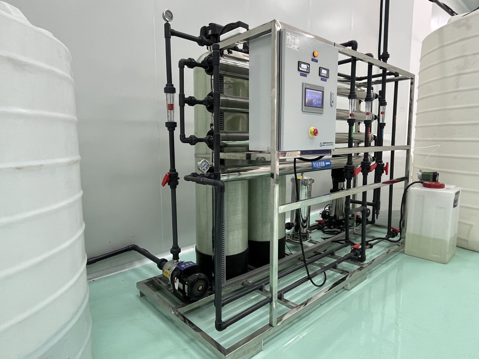
- First and second pass reverse osmosis with membrane degassing between passes
- Continuous EDI stacks replacing acid / alkali regenerated mixed beds
- 185 nm UV oxidation, polishing resin and 0.22 μm terminal filtration
- 316L polished recirculation loop feeding every rinse station
Results
Outcome On Site
Stable 18.2 MΩ·cm resistivity at all use points
Regeneration chemicals and waste eliminated entirely
Unattended automatic operation with online quality logging
Site Photos
Installation Gallery